At the heart of the Asus EN8800GTS/HTDP/320M videocard is nVidia's 'G80' GPU, built
on TSMC's 90 nanometer manufacturing process. The Geforce 8800GTS GPU contains 681 million
transistors, by way of comparison the Geforce 7800GTX 'G70' had 302 million transistors.
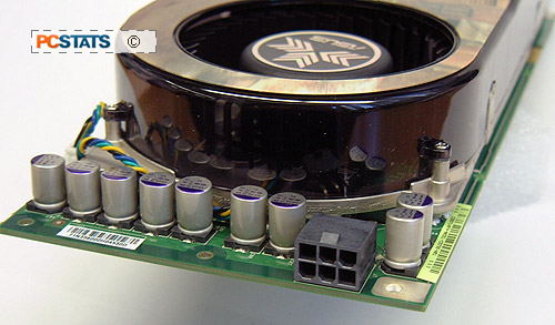
In its current form nVidia's 'G80' demands a lot of power and generates a lot
of heat. The GPU puts out upwards of 80W-85W under load. This is why the
reference videocard design utilizes such a large heatpipe cooled thermal
solution.
More
importantly than transistor counts and power output is that nVIDIA's
'G80' is the first DirectX 10 compatible GPU-series on the market, and it is
completely different from videocards of the past. The 'G80' utilizes a unified
architecture, which is another way of saying that it merges vertex and pixel
shaders into one floating point processor. There have been other GPUs to take
this route, notably the ATi graphics processor inside the Xbox 360, but nVIDIA
is first to release this type of technology for the home PC.
The
GeForce 8800GTS is based on the same G80 core that powers the GeForce 8800GTX,
however nVIDIA disables a few rendering pipelines here and there, and trims the
memory bus to ensure that the GeForce 8800GTS is slower than the GTX. It's not
as bad as it sounds, the GeForce 8800GTS 320MB videocard is still a wickedly
fast platforms for games.
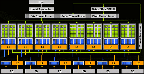
GeForce 8800GTX Core Shown
The
nVIDIA GeForce 8800GTS GPU has access to six "Thread Processors" as opposed to
eight with the GeForce 8800GTX. Each has 16 Stream Processors (SP), for a total
96. Gone are the hard coded Vertex and pixel shaders, they have been
replaced with the more flexible Stream Processor that calculates both types of
data. The Stream Processors run at a blistering 1.35 GHz. Traditional core clock
speeds as we know it are dead, as several internal processors are running at
different speeds.
Each
Thread Processor has two groups of eight SP, and each group talks to an
exclusive texture address filter unit as well as well as being connected to the
shared L1 cache. When more memory is needed the Thread Processor connects to the
crossbar memory controller. nVIDIA's crossbar memory controller is broken up
into five 64 bit chunks (six with the GeForce 8800GTX), which means the width is
essentially 320 bits wide (384 bits for the 8800GS).
 By moving the GPU
towards a threaded design, the nvidia G80 is much more like a processor than any
graphics cores of the past. Any type of data, be it pixel, vertex, or geometry
shader can be processed within the SP. This allows load balancing to occur
between the various tasks.
By moving the GPU
towards a threaded design, the nvidia G80 is much more like a processor than any
graphics cores of the past. Any type of data, be it pixel, vertex, or geometry
shader can be processed within the SP. This allows load balancing to occur
between the various tasks.
Although
DirectX 9 does not support unified shader instructions, load balancing is
handled automatically by the GPU so it's not something developers have to worry
about. Load balancing ensures optimal performance from the GPU no matter what
the situation, as pixel and vertex processing shifts greatly during game play.
While
there are 96 Stream Processors broken down into 16 8-section chunks, there are
only 32 texturing units total, 4 per thread processor. The texturing units run
at core clock speed, and as indicated can handle 32 textures per clock. One of
the most important "features" is that the texture unit operates independently of
the SP, so texturing can occur at the same time as shader rendering.
One other
new feature the G80 brings to the table is a stand alone video display engine
completely designed for this GPU generation. Set off to the left of the 'G80' GPU
is nVIDIA's new discrete display chip. This chip supports both TDMS logic for
LCD monitors and RAMDACs for analog displays. By moving the display engine
outside the GPU, it allows nVIDIA to have less overhead with multi-GPU
videocards.
nVIDIA PureVideo and High
Definition Content
 High definition is
the future entertainment standard of tomorrow's video's. Playing high definition
content on current generation PCs can bog down even the fastest processors
because there is more data to handle. Similar to the need for DVD accelerators a
few years ago, nVIDIA PureVideo enables computer users to view MPEG-2/DVD and
WMV9 High Definition formats on the monitor without slowing the system to a
crawl.
High definition is
the future entertainment standard of tomorrow's video's. Playing high definition
content on current generation PCs can bog down even the fastest processors
because there is more data to handle. Similar to the need for DVD accelerators a
few years ago, nVIDIA PureVideo enables computer users to view MPEG-2/DVD and
WMV9 High Definition formats on the monitor without slowing the system to a
crawl.
The
PureVideo standard incorporates a hardware accelerator for the afore mentioned
MPEG-2/DVD, and Microsoft Windows Media High Definition Video standards (WMV9
HD). According to nVIDIA's documentation on PureVideo, the GPU (GeForce 6, 7 and
8 series GPUs) takes on video decoding tasks from the CPU, and the end result is
smoother, shutter free High Definition playback. nVIDIA PureVideo also supports
most current and future high definition formats.
PureVideo
is more than just a media accelerator; it also includes features to improve
video picture quality. DVD, cable and satellite video provide poor crispness,
clearness and smoothness that consumers have been desperate to be "saved from."
nVIDIA's PureVideo technology applies spatial temporal de-interlacing to
apparently deliver a better image than traditional de-interlacing can muster.
PureVideo
also fixes the 3:2 pull down problem that can arise from 24 fps video being
converted to 30 fps for viewing on TVs or monitors. By recovering the original
24 frame content, PureVideo allows for a clear crisper image.
Examining CPU Load with
PureVideo
To test
PureVideo's High
Definition accelerating capabilities on the Asus EN8800GTS/HTDP/320M, PCSTATS
will play back a video downloaded from Microsoft's WMV HD Content Showcase through Windows Media Player 10. "The
Discoverers" (IMAX) video is available in both 720P and 1080P formats. AMD
processor utilization will be monitored via Task Manager.
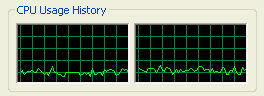
When playing the 720P version of the Discoverers video the
CPU usage jumped between 15-20% which is pretty good. That leaves a lot of
resources for background tasks.
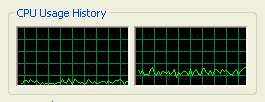
CPU usage when running the 1080P version of the Discoverers video was even lower, usage stayed
between 11-17%! That's great, with a videocard like the Asus EN8800GTS/HTDP/320M, you don't
have to worry about running high definition videos. Next up, overclocking
the Asus EN8800GTS/HTDP/320M videocard!