The four execution cores you find in the Intel Core i5
700-series and the Core i7 800-series ("Lynnfield", just in case you forgot) are
largely identical to those found in the Core i7 900-series ("Bloomfield") of
processors.
All three lines of processors use Intel's "Nehalem"
architecture, so they have 32KB of L1 cache and 256KB of L2 cache per core, and
a large 8MB L3 cache that's shared between the four physical cores. All Intel
"Nehalem" processors also have improvements in branch prediction and
instruction decoding, which make them a bit faster clock-for-clock when compared
to Intel's Core 2 Duo processors.
The Core i5 750 processor, along with Intel's Core i7
860 and Core i7 870 processors consist of 774 million transistors, occupying a
296mm2 die. This actually makes the die a little larger than Intel's Core i7
900-series of "Bloomfield' processors (731 million transistors, 263mm2 die). The
extra size is due to the embedded PCI Express controller that makes up the
"uncore" of the Intel Core i5 700-series and Core i7 800-series of processors.
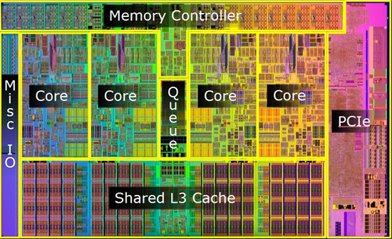
Intel Uncore Explained
An "uncore" is all the bits on the processor die that
aren't the core. If you look at the "Lynnfield" die shot above, there are four
cores, a queue and 8MB of shared L3 cache which make up the "core" of the chip.
It's surrounded by the "uncore", which in this case consists of the PCI Express
and memory controllers.
Having a memory controller integrated onto the CPU die
isn't a new concept. AMD has been doing it for years with its socket AM2
processors, and Intel followed suit when it launched the Core i7 900-series of
processors in late 2008. Moving to an on-die controller not only allowed the
processor direct access to memory, it also eliminated the bottleneck-prone Front
Side Bus.
The memory controller for Intel's Core i7 800-series and
Core i5 750-series is similar to the memory controller in a Core i7 900-series
processor, but it's been modified to be more cost-effective. Like the Core i7
900-series ("Bloomfield"), it's still DDR3-exclusive, but these new processors
now use more conventional dual-channel memory instead of triple-channel memory.
To compensate for the reduction in channels the official supported memory speed
has been increased to DDR3-1333MHz clock speeds. While this cost-cutting has
some impact on theoretical bandwidth capabilities and synthetic benchmarks, for
most real-world usage scenarios you won't notice the difference.
Intel's Core i7 800-series and Core i5 700-series
processors takes the "uncore" a step further, and in addition to the memory
controller there are also 16 PCI Express 2.0 lanes now integrated onto the die
of the CPU.
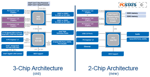
The changes to the PCI Express graphics sub-system won't
have a huge impact on buyers, most P55 motherboards will still have three PCI
Express slots that can be run in (x16/x4) or (x8/x8/x4) mode, the only
difference is that now the first two slots will be handled directly by the CPU,
which will have the nice side effect of removing some system latency.
Future generations of Intel processors will integrate a
graphics processor onto the CPU die as well, moving even closer to a true
"system on a chip" design, where a single CPU chip will control every aspect of
your computing. That one's still a few years down the line, but rest assured
that PCSTATS will be keeping you up to date as the industry moves forward.
Processor Thermal Design Power (TDP) and Turbo Boost
Since the Core i5 700-series and Core i7 800-series
"uncore" now has two controllers on it and the die size has grown, you'd be
forgiven if you thought that their power consumption and TDP would have grown
accordingly. This isn't the case.
The thermal design power (TDP) of Intel's Core i5
700-series and Core i7 800-series of processors is rated at a mere 95W. This is
a huge reduction in power consumption when compared to the 130W TDP of Intel's
Core i7 900-series processors. Such low power consumption and heat production
mean that these CPUs have a lot of headroom for overclocking... and Intel has
taken that into account with Turbo Boost.
Turbo Boost is an automatic, per-core overclocking
scheme that takes advantage of "Lynnfield"'s low TDP. Through the use of an
on-die thermal microcontroller, the processor can monitor how many cores are
currently being put under load, how much heat and power they're using, and
automatically adjust speeds to match.
The amount of overclocking you get from Turbo Boost
depends on which processor you have, how many cores are being put under load,
and the current temperature of the processor. The Intel Core i5 750 processor
being used in this review has a base speed of 2.66GHz. With three or four cores
active it can Turbo Boost up to 2.8GHz, and with one or two cores active it can
Turbo boost up to 3.2GHz.
Turbo Boost is the great equalizer that bridges the gap
between dual-core and quad-core performance. Dual-core processors have typically
been able to reach higher speeds than quad-cores, because more cores drew extra
power and generated extra heat, limiting clockspeeds. This made dual-cores
better suited for gaming and other single-threaded tasks, while quad-cores
tackled highly parallel tasks like video encoding. Intel's "Lynnfield"
processors change all of this, delivering intelligent overclocking that balances
performance based on need.
Of course, the Core i5 750 processor can still be
overclocked the traditional way as well, PCSTATS will be getting to that in just
a page or two. For now though, let's take a look at how much juice an Intel Core
i5 system really uses...