PCSTATS     
[X]   Directory of
Guides & Reviews

Beginners Guides
Motherboards by Brand
Weekly Newsletter
Archived Newsletters

Sparkle GTX260 Core 216 GeForce GTX 260 Videocard Review
Sparkle GTX260 Core 216 GeForce GTX 260 Videocard Review - PCSTATS
The Geforce GX 260 core on Sparkle's videocard is clocked at the default speed of 576MHz, the shaders hum away at 1242MHz, while the GDDR3 memory runs at an even 999MHz.
 81% Rating:   
Filed under: Video Cards Published:  Author: 
External Mfg. Website: Sparkle May 26 2009   J. Apong  
Home > Reviews > Video Cards > Sparkle GTX260 Core 216

nVidia Geforce GTX260 and the GT200 GPU

The 
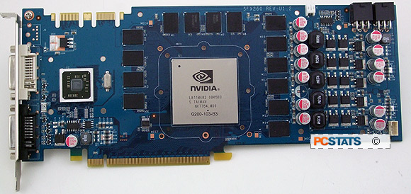
Sparkle GTX260 Core 216 videocard opts for nVidia's default core and memory clock speeds, rather than pre-overclocking anything at the factory. Thus the 55nm Geforce GTX260 GPU runs at 576MHz, the 896MB of GDDR3 memory at 999MHz and the 216 shader processors at 1242MHz. That translates into roughly 715 GFLOPS of processing power, nice.

To understand 
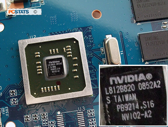
where all this power comes from, we need to take a look at the nVidia GeForce GTX260 GPU - a massive monolith of an IC sheathed behind its heatspreader. Code named 'GT200', this graphics processor is actually the second revision nVidia has made to its new next-generation graphics processors.

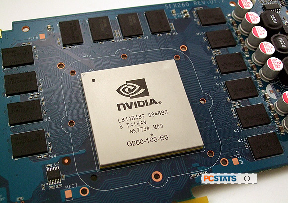
The nVidia GT200 GPU chip is designed with 240 total shader processors. Each one is a tiny processor that can compute either pixel or vertex mathematical operations. The processors are designed to operate on graphical information simultaneously, with each shader processor is operating on a single pixel per cycle.

These shader processors are broken up into clusters of 24, called Texture/Processor Clusters. In addition to the shader processors, the clusters also include a texturing array and a geometry controller. While the high end nVidia Gefore GTX 280 graphics card has all 10 of the GT200's TPCs enabled, the original Geforce GTX 260 had only 8 of the 10 TPCs enabled, the remaining two are either disabled or had defects that caused them to fail in nVidia's quality assurance testing.

The Sparkle GTX260 Core 216 videocard that PCSTATS is tested today actually has an additional TPC enabled, so there are 9 clusters of 24 shader processors, for a total of 216 shader processors. This translates into a bit of extra shader muscle and texturing savvy. The GT200 GPU is oriented around shader processing and calculation, designed for games that utilize intense special effects like high dynamic range lighting, geometry distortion and dynamic reflections.

In addition to the increased shader cores, nVidia has also managed to get the GT200 GPU's 1.4 billion transistors shrunk down to a 55nm process. While the original 65nm GT200 die was a massive 576mm2, the die-shrink brings the overall die size down to 487mm2. Shrinking the overall size of the chip influences power consumption, heat output and of course price.


This small chip is the nVidia video output controller (NVIO2-A2). It controls HD video acceleration functions, as well as high-definition content protection (HDCP), necessary for playing Blu-Ray discs and other HD media.

Looking at the naked Sparkle Geforce GTX260 videocard makes one point very clear; nVidia's GT200 processors are big. At the time it was produced, nVidia's 65nm GT200 GPUs were the biggest processor dies that the Taiwan Semiconductor Corporation ever fabricated.


The videocard has two SLI connectors so it can be paired with either one or two additional Geforce GTX260 cards.

The SParkle GTX260 Core 216 videocard can, of course, be hooked up in SLI. The Geforce GTX 260 can be configured to work in two way or three-way SLI mode, with each videocard splitting the graphics load between them to increase frame rates when more graphical options are turned on. To run in SLI mode, you need a motherboard based on a compatible nVidia nForce chipset or an SLI-certified version of Intel's X58 chipset, and a pair of Geforce graphics cards based on the same GPU.

PCSTATS will be overclocking the Sparkle GTX260 videocard next, but first it's time for a little power consumption testing, then it's onto the benchmarks you've been waiting for!

< Previous Page © 2023 PCSTATS.com Next Page >


Contents of Article: Sparkle GTX260 Core 216
 Pg 1.  Sparkle GTX260 Core 216 GeForce GTX 260 Videocard Review
 Pg 2.  — nVidia Geforce GTX260 and the GT200 GPU
 Pg 3.  Videocard Power Consumption Measurements
 Pg 4.  Overclocking a Geforce GTX260 with nVidia nTune
 Pg 5.  Videocard Benchmarks: 3DMark06
 Pg 6.  DX10 Videocard Benchmarks: 3DMark Vantage, STALKER, Crysis
 Pg 7.  DX10 Videocard Benchmarks: Call of Juarez
 Pg 8.  DX10 Videocard Benchmarks: Lost Planet
 Pg 9.  Videocard Benchmarks: FEAR
 Pg 10.  AA/AF Videocard Benchmarks: FEAR AA/AF
 Pg 11.  AA/AF Videocard Benchmarks: FarCry 2, Crysis
 Pg 12.  Radeon or Geforce GTX260 - Who's the better GPU?

 
Hardware Sections 


PCSTATS Network Features Information About Us Contact
FrostyTech
PCSTATS Newsletter
Tech Glossary
Technology WebSite Listings
News Archives
(Review RSS Feed)
Site Map
PCstats Wallpaper
About Us
Privacy Policy
Advertise on PCSTATS

How's Our Driving?
© Copyright 1999-2023 www.pcstats.com All rights reserved. Privacy policy and Terms of Use.